A couple of days back, Ganesh Venkataramanan, leader of the Tesla Dojo project, announced the Dojo machine learning training system. It’s an unusually network rich, power dense, and memory light design. I’ve summarized the architecture of the system below but I found three aspects of the system particularly interesting:
- Massive Network: Each D1 chip delivers 16,000 GBps (4 channels of 4Tbps) of networking and they are combined into 25 chip MCM (Multi-Chip Modules) to deliver 36,000 GBps (4x 9TBps) of network bandwidth
- Tiny Memory to compute ratio: Each D1 chip is made up of 354 functional units and each functional unit has only 1.25 MB of SRAM and no DRAM at all so there is less than ½ GB of memory per D1 processor. They have provisioned large DRAM pools on each end of a 5 rack row there is no DRAM in the compute racks themselves. In thinking through how they can operate so light on memory, I suspect it’s a combination of vast networking bandwidth and that the system is designed to run vision models where are less memory intensive than many other common ML training workloads.
- Massive power density: Each D1 chip only dissipates 400 W which about as expected for a modern part of that size but they have combined these into fairly dense 25 chip MCMs called training tiles each of which dissipates 15kw (10kw of D1s and 5kw of voltage regulators and other overhead). That’s 1.8 megawatts for the full planned 10 rack Dojo training system. As a point of scale a mid-sized datacenter will run in the 30 to 40 megawatt range).
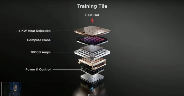
Looking closely at the pictured roughly 1 sq ft training tile above, the top is an aluminum plate presumably to mate up against a phase change liquid cooling system.
It’s a minor point but it’s a nice touch to put the VRDs( Voltage Regulator Down) directly on tile allowing them to deliver an unusually high 52V to power the tile. Given the 15kW draw, that’s still a 288A draw at 52V.
354 Functional units are combined in a single 645 mm^2 D1 chip. 25 D1 chips form a multichip module called a training tile and 12 training tiles form a rack and 10 racks for an Exapod.
Functional Unit:
- 4 thread SMT (Symmetric Multi Thread)
- 512 GBps (4x 128 GBps) network bandwidth
- 1.25MB SRAM
- SIMD matrix unit
D1 Chip: 645mm^2
- 354 Functional Units (training nodes) per D1
- 16,000 GBps (4x 4TB) network bandwidth
- 442.5 MB SRAM
- 2Ghz
- 400W (fairly low)
Training Tile: ~1 sq ft
- 25 D1 Chips
- 36,000 GBps (4x 9TB) network bandwidth
- 11GB SRAM/tile
- VRD on wafer with 52VDC input
- Full mechanicals to manage 15kW
- 10kW from 25 D1s and 5kW from VRDs and other overhead)
Cabinet (rack):
- 12 Training Tiles per rack (2 trays of 6 per tray)
- 132GB SRAM/rack
- 180kW/rack
Exapod: 10 racks
- Still full 36TBps between each module
- Each 5 rack pod has general purpose CPUs on either side with large DRAMs pools
- 4 DRAM pools on full 2 row, 10 rack Exapod
- 1.32TB SRAM/Exapod
- 1.8MW per Exapod
It’s quite an innovative system. More details at: Tesla’s AI Chip Revealed