For years I’ve been saying that, as more and more workloads migrate to the cloud, the mass concentration of similar workloads make hardware acceleration a requirement rather than an interesting option. When twenty servers are working on a given task, it makes absolutely no sense to do specialized hardware acceleration. When one thousand servers are working on the task, it certainly makes sense to do custom boards and/or Field Programmable Gate Arrays (FPGAs). But one thousand is actually a fairly small number in the cloud. When there might several hundred thousand servers all running the same workload, hardware specialization goes from an interesting idea to almost a responsibility. Hardware acceleration can reduce latency by a factor of ten, decrease costs by a factor of ten and, it’s better for the environment, with power/performance improved by at least a factor of ten.
In the 80s I argued that specialized hardware was crazy and the future of our industry was innovative software on low-cost, commodity, general-purpose processors. For many decades that certainly appeared to be true and I’ve managed to make a respectable living on that basic approach: improving performance, availability, and lowering costs by using large numbers of commodity processors. If I ever was correct on this point, it’s certainly not true any longer. We are entering the era of hardware acceleration.
In actuality hardware acceleration has been around in large numbers for a considerable length of time. Commercial routers have massive Application Specific Integrated Circuits (ASIC) at the core. Many specialized network appliances have workload specialize hardware doing the heavy lifting. Most network Interface cards have ASICs at the core. The most effective BitCoin mining engines are using hardware workload acceleration in custom ASICs.
It really wasn’t that long ago that that X86 processors didn’t include floating point on die and it was either done in software on in a separate floating point co-processor. In the somewhat more distant past, I’ve worked on processors that even lacked a fixed point multiply instruction. In the early days of high-performance computing, matrix work was done in software. Cray moved it into hardware with the Cray 1 vector units and, as the cost of a transistor continues to plummet, even hardware vector units are now standard fare in a modern X86 processor.
Hardware acceleration isn’t new, but the operations being accelerated are moving up from the incredibly primitive to replacing ever larger hot kernels of higher-level applications. In the early days, adding the MultiplyAdd (also called Fused-Multiply Add or fmadd) instruction to IBM POWER was a reasonably big deal in allowing the two operations to be done as a single instruction rather than as two. Over time, more hardware accelerations like cryptography have been creeping into general purpose processors and I expect this process will not just continue but pick up pace. General purpose processors have the die real estate to spare and, even if the accelerators are used rarely, with 10x gains across many dimensions, hardware acceleration makes excellent economic sense. In fact, as Moore’s law slows, higher-level hardware acceleration will become one of the most important ways that the next processor generation shows material advantage over the previous.
While general purpose processors will continue to get more higher–level accelerations, another trend emerging much more broadly over the last ten years is the offloading of important workloads from the general-purpose processor entirely. Where a workload has both high value and massive parallelism, it’s a candidate for migration off of general purpose processors and onto graphics processors. It turns out the massive parallelism required for advanced computer graphics also supports some non-graphical workloads incredibly well. Some of the first examples I came across was the offloading of hot financial calculations and the acceleration of seismic studies used in oil exploration. These were important, but the golden workload that has absolutely exploded the general purpose graphics processor market is machine learning. Training neural networks is a highly parallel task that runs incredibly well on graphics processors. Five years ago there was lots of talk about this and some were doing it. Today, it’s hard to justify not running these workloads on General Purpose Graphics Processor Units (GPGPUs) once the workload is being run at scale.
As an example, the Nvidia Tesla K80 GPGPU board has 2 sockets with 2496 CUDA cores each and the overall system is capable of 8.74 TFLOB. The individual cores aren’t that powerful nor amazingly fast but, if the workload is highly parallel, there are a lot of cores available to host it. This part is a bit power intensive at 300W TDP (thermal design power) but that’s not really a problem. What’s both a massive problem and proof of how well this systems supports some workloads is the price. The retail price of the K80 when announced was $5,000. This board is just about as close as our industry gets to pure profit margin with a complete disregard to cost so large discounts are available. But, regardless of discount, this board will never be confused for a low-cost or commodity part.
The good news is our industry is self-correcting and there are many new solutions under development. In fact, partly because the price of this part is so crazy high and partly because cloud volumes are now large enough to justify customer processors, we are going to see more and more workloads hosted on custom ASICs. 15% of the 2016 ISCA papers were on machine learning hardware accelerators and Google, Microsoft, and Amazon all have digital design skills. Not much has been written about the semiconductor work done by the mega-providers but, as an example, at AWS we deploy many hundreds of thousands of custom ASICS each year.
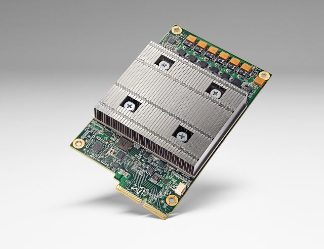
I just read about another excellent example higher-level application acceleration. In fact this best example I’ve seen publicly disclosed so far. The paper “In-Datacenter Performance Analysis of a Tensor Processor Unit” will be presented at the upcoming 44th International Symposium on Computer Architecture (ISCA) to be held in Toronto Canada June 26, 2017.
In my opinion, this is excellent work, a well-written paper, and a balanced analysis of what they produced and started to deploy back in 2015. It’s the normal practice in our industry to only show that which has already been replaced or is about to be replaced but that’s just the reality of commercial innovation and I do the same thing myself.
What I found most striking is the elegant simplicity of what has been done. It wins over general purpose Intel processors and Nvidia GPGPUs of the same generation by the greater than 10x we would expect and yet, they have kept the part simple and shown good taste in what to include and what not to. The paper uses power/performance as a proxy for the price/performance they know they should be using but since this is commercial innovation, pricing needs to remains confidential.
Because the part and board have been in production since 2015, they will have likely done more than 10^6 volume by now. Since the volume is good by semiconductor standards and the part is not that complex, I would speculate that the part is less than $50 and the full PCIe board will cost under $100. For machine learning inference, this part is more than an order of magnitude faster than an Nvidia GPGPU while being more than an order of magnitude less expensive. This is the power of workload hardware specialization and we are going to see a lot more of this over the next decade.
Some key speeds and feeds from the paper:
- 65,536 8-bit Multiply-Accumulate matrix multiply unit
- 92 TeraOps/second
- 28 MiB software-managed on-die memory
- 15x to 30x faster than contemporary GPU (Nvidia K80) or CPU (Haswell)
- 30x to 80x higher TeraOps/second/watt than CPUs or GPGPUs
- System is actually memory bound on four of the six neural net applications so the next part, if you assume improvements at roughly the same speed as CPUs and GPGPUs, would achieve a 70x the performance/watt of the comparable GPGPU and 200x with the comparable CPU
Some interesting observations and lessons learned from the paper in bold with my short form notes in italics:
- Fallacy: NN inference applications in datacenters value throughput as much as response time: Machine learning training values throughput but most inference applications are customer facing where response time is a primary concern.
- Fallacy: The K80 GPU architecture is a good match to NN inference: The K80 and the shorter word length K60 are good but expensive hosts for training. For inference they are only marginally better than general purpose CPUs so their high costs ends up dominating.
- Pitfall: Architects have neglected important NN tasks: 15% of the 2016 ISCA papers were on Neural Net accelerators further underlining my point above. This underlines my point that the solution to the GPGPUs are coming soon.
- Pitall: For NN hardware, Inferences Per Second (IPS) is an inaccurate summary performance metric: Our results show that IPS is a poor overall performance summary for NN hardware, as it’s simply the inverse of the complexity of the typical inference in the application (e.g., the number, size, and type of NN layers).
- Fallacy: The K80 GPU results would be much better if Boost mode were enabled: Setting aside the negative impact of K80 Boost mode on TCO (Section 3), we measured it on LSTM1. Boost mode increased the clock rate by a factor of up to 1.6—from 560 to 875 MHz—which increased performance by 1.4X, but it also raised power by 1.3X. The net gain in performance/Watt is 1.1X, and thus for LSTM1, boost mode would have a minor impact on our energy-speed analysis.
- Fallacy: CPU and GPU results would be comparable to the TPU if we used them more efficiently or compared to newer versions: We originally had 8-bit results for just one DNN on the CPU, due to the significant work to use AVX2 integer support efficiently. The benefit was ~3.5X. It was less confusing (and space) to present all CPU results in floating point, rather than having one exception, with its own roofline. If all DNNs had similar speedup, performance/Watt ratio would drop from 41-83X to 12-24X. The new 16-nm, 1.5GHz, 250W P40 datacenter GPU can perform 47 Tera 8-bit ops/sec, but was unavailable in early 2015, so isn’t contemporary with our three platforms. We also can’t know the fraction of P40 peak delivered within our rigid time bounds. If we compared newer chips, Section 7 shows that we could triple performance of the 28-nm, 0.7GHz, 40W TPU just by using the K80’s GDDR5 memory (at a cost of an additional 10W).
- Pitfall: Performance counters added as an afterthought for NN hardware: 106 performance counters were not enough.
- Fallacy: After two years of software tuning, the only path left to increase TPU performance is hardware upgrades: More yet remains to be done in the compiler to further support the part but I’ll still bet a new TPU is coming soon if not already in production.
This is really fine work by Norman Jouppi, Cliff Young, Nishant Patil, the always excellent David Patterson, and others. If you can find the time, go ISCA2017 in Toronto and, for sure, read the paper: In-Datacenter Performance Analysis of a Tensor Processing Unit.